")
")

")
![]() Service
Service
Over the years, we provided a great number of domestic and foreign electronic manufacturers with professional design services, many of them are well-known international brands, their strict design requirements and a variety of design types, training Palpilot engineers profound design skills, whether high density multi-layer board, high-speed signal board, mixed signal board, blind buried hole board, we are competent to handle all the difficult cases.
![]() Advantage
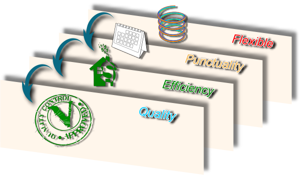
Advantage
![]() Design Data
Design Data
| 零件 | SPEC | 建立零件需參照零件 SPEC 中的尺寸圖及 Layout 建議圖進行建置。 |
| Rule | 如零件建立有非標準零件 SPEC 中標示的尺寸變更需求時,需請提供相關 零件建立的 Rule。 | |
| Placement | DXF | 機構圖中需標示 Outline 及哪些固定式機構零件及機構中的各別高度標示及零件/走線禁止區。 |
| 線路圖 | 配置零件時需依照線路圖進行相關電路零件位置配置。 | |
| Guide | 當有電路希望配置的方向或位置甚至相關零件配置的要求時,需請提供相關作業 Rule。 | |
| Stack-up | 零件配置需思考走線空間利用及後續提供 3D 資料給機構做 Confirm,需請提供板中的堆疊及厚度。 | |
| Route | DXF | 機構圖中需標示 Outline 及哪些固定式機構零件及機構中的各別高度標示及零件/走線禁止區。 |
| 線路圖 | 走線時需依照線路圖進行相關電路調整及配線。 | |
| Guide | 當有走線樣式、等長誤差、各別電路的走線要求時,需請提供相關 Layout Rule。 | |
| Stack-up | 因走線思考空間利用需要,需請提供板中的堆疊及阻抗表 (板中線路使用的阻抗線寬/spacing)。 | |
| Silk | Guide | 是否板中有版本、板號、環保標章、Logo 等標示及文字白漆尺寸大小、方向等要求。 |
| Gerber | Guide | 由於各家的出圖 Rule 及檔案配置都不盡相同,建議您提供過去的參考範例,以利整理為貴方需求的 Gerber File。 |
![]() Applications
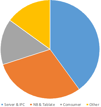
Applications
![]() Design Flow
Design Flow
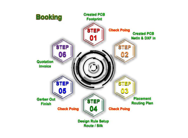
We provide customers full-process service with component set up, constrain, placement, routing, silkscreen and Gerber out. In addition, we also provide a simple routing service.